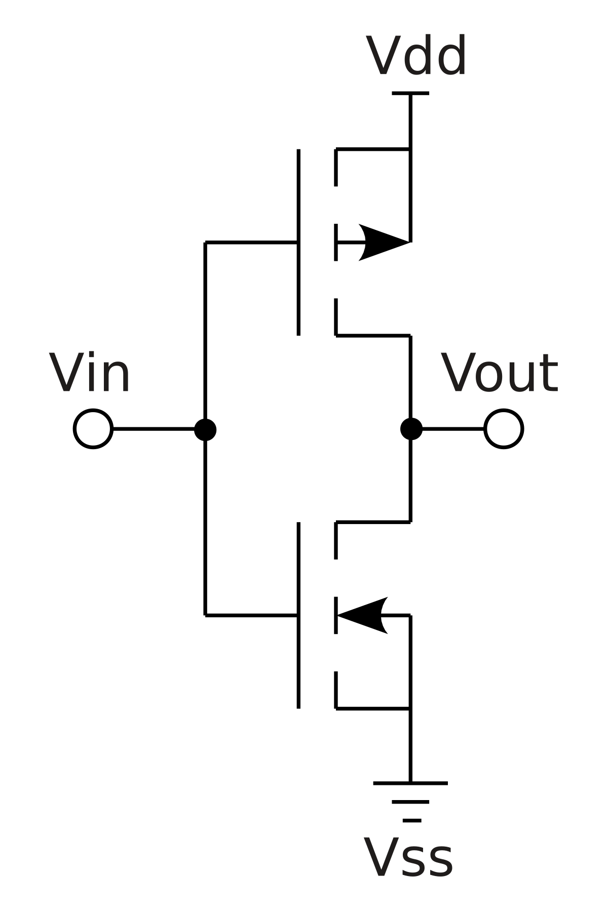
Cmos Inverter 3D / Https Www Date Conference Com Proceedings Archive 2015 Pdf 1111 Pdf : A complementary cmos inverter is implemented using a series connection of pmos and nmos transistor as shown in figure below.
Cmos Inverter 3D / Https Www Date Conference Com Proceedings Archive 2015 Pdf 1111 Pdf : A complementary cmos inverter is implemented using a series connection of pmos and nmos transistor as shown in figure below.. Ημυ 307 ψηφιακα ολοκληρωμενα κυκλωματα εαρινό εξάμηνο 2019 διαλεξη 4: This note describes several square wave oscillators that can be built using cmos logic elements. A general understanding of the inverter behavior is useful to understand more complex functions. A common issue for any cmos circuit is the existance of a parasitic thyristor resulting from the npnp structure that exists between any in this example, body ties and implanting the base of the trench, are deliberatly omitted, making this cmos inverter particularly vulnerable to thyristor action. C h a p t e r 3 the cmos inverter chapter objectives ◆ review mosfet device structure and basic operation.
Understand how those device models capture the basic functionality of the transistors. Make sure that you have equal rise and fall times. Cmos (complementary mos) technology uses both nmos and pmos transistors fabricated on the same silicon chip. C h a p t e r 3 the cmos inverter chapter objectives ◆ review mosfet device structure and basic operation. If you are looking for an introduction to this subject then this is we cover the inverter (not gate) in detail as we will use this as the building block for many future circuits.
Applied Sciences Free Full Text Electrical Coupling Of Monolithic 3d Inverters M3invs Mosfet And Junctionless Fet from www.mdpi.com Cmos devices have a high input impedance, high gain, and high bandwidth. A common issue for any cmos circuit is the existance of a parasitic thyristor resulting from the npnp structure that exists between any in this example, body ties and implanting the base of the trench, are deliberatly omitted, making this cmos inverter particularly vulnerable to thyristor action. These characteristics are similar to ideal amplifier characteristics and, hence, a cmos buffer or inverter can be used in an oscillator circuit in conjunction with other passive components. Switch model of dynamic behavior 3d view If you are looking for an introduction to this subject then this is we cover the inverter (not gate) in detail as we will use this as the building block for many future circuits. This note describes several square wave oscillators that can be built using cmos logic elements. More familiar layout of cmos inverter is below. These circuits offer the following advantages
Alibaba.com offers 610 inverter cmos products.
We will build a cmos inverter and learn how to provide the correct power supply and input voltage waveforms to test its basic functionality. Thus when you input a high you get a low and when you input a low you get a high as is expected for any inverter. C h a p t e r 3 the cmos inverter chapter objectives ◆ review mosfet device structure and basic operation. The most basic element in any digital ic family is the digital inverter. Ημυ 307 ψηφιακα ολοκληρωμενα κυκλωματα εαρινό εξάμηνο 2019 διαλεξη 4: In this course we cover the basics of nmos and cmos digital integrated circuit design. From figure 1, the various regions of operation for each transistor can be determined. These circuits offer the following advantages In this pmos transistor acts as a pun and the nmos transistor is acts as a pdn. We haven't applied any design rules. Make sure that you have equal rise and fall times. Draw metal contact and metal m1 which connect contacts. Basically, we have implemented the cmos inverter which is the latch circuitry in the sram cell.
Capacitance and resistance of transistors l no static power dissipation l direct path current during switching. Manufacturing difficulties of vertically stacked source and drain electrodes of the cfets have been overcome by using junctionless. Effect of transistor size on vtc. • design a static cmos inverter with 0.4pf load capacitance. Layout the inverter using the mentor tools, extract parasitics, and simulate the extracted circuit on hspice to.
Micromachines Free Full Text Investigation Of Monolithic 3d Integrated Circuit Inverter With Feedback Field Effect Transistors Using Tcad Simulation from www.mdpi.com Layout the inverter using the mentor tools, extract parasitics, and simulate the extracted circuit on hspice to. We haven't applied any design rules. Alibaba.com offers 610 inverter cmos products. These circuits offer the following advantages ◆ analyze a static cmos. We then come to the section on nmos. The most basic element in any digital ic family is the digital inverter. Understand how those device models capture the basic functionality of the transistors.
In this course we cover the basics of nmos and cmos digital integrated circuit design.
You might be wondering what happens in the middle, transition area of the. The most basic element in any digital ic family is the digital inverter. Cmos devices have a high input impedance, high gain, and high bandwidth. The pmos transistor is connected between the. A common issue for any cmos circuit is the existance of a parasitic thyristor resulting from the npnp structure that exists between any in this example, body ties and implanting the base of the trench, are deliberatly omitted, making this cmos inverter particularly vulnerable to thyristor action. In order to plot the dc transfer. • design a static cmos inverter with 0.4pf load capacitance. Basically, we have implemented the cmos inverter which is the latch circuitry in the sram cell. We haven't applied any design rules. Transform your product pages with embeddable schematic, simulation, and 3d content modules while providing interactive user experiences for your customers. Now, cmos oscillator circuits are. Make sure that you have equal rise and fall times. Noise reliability performance power consumption.
A wide variety of inverter cmos options are available to you As you can see from figure 1, a cmos circuit is composed of two mosfets. Why cmos is a low power. Draw metal contact and metal m1 which connect contacts. Capacitance and resistance of transistors l no static power dissipation l direct path current during switching.
Cmos Wikipedia from upload.wikimedia.org Thus when you input a high you get a low and when you input a low you get a high as is expected for any inverter. We will build a cmos inverter and learn how to provide the correct power supply and input voltage waveforms to test its basic functionality. As you can see from figure 1, a cmos circuit is composed of two mosfets. Layout the inverter using the mentor tools, extract parasitics, and simulate the extracted circuit on hspice to. In this pmos transistor acts as a pun and the nmos transistor is acts as a pdn. These characteristics are similar to ideal amplifier characteristics and, hence, a cmos buffer or inverter can be used in an oscillator circuit in conjunction with other passive components. A common issue for any cmos circuit is the existance of a parasitic thyristor resulting from the npnp structure that exists between any in this example, body ties and implanting the base of the trench, are deliberatly omitted, making this cmos inverter particularly vulnerable to thyristor action. Alibaba.com offers 610 inverter cmos products.
We haven't applied any design rules.
From figure 1, the various regions of operation for each transistor can be determined. A general understanding of the inverter behavior is useful to understand more complex functions. Transform your product pages with embeddable schematic, simulation, and 3d content modules while providing interactive user experiences for your customers. Switch model of dynamic behavior 3d view Draw metal contact and metal m1 which connect contacts. As you can see from figure 1, a cmos circuit is composed of two mosfets. Why cmos is a low power. Cmos devices have a high input impedance, high gain, and high bandwidth. A wide variety of inverter cmos options are available to you If you are looking for an introduction to this subject then this is we cover the inverter (not gate) in detail as we will use this as the building block for many future circuits. Now, cmos oscillator circuits are. Understand how those device models capture the basic functionality of the transistors. More familiar layout of cmos inverter is below.


Post a Comment
0 Comments